 Scientists at IBM Research and the California Institute of Technology announced today (Aug. 17) a scientific advancement that can enable the semiconductor industry to pack more power and speed into tiny computer chips. It also can help chip makers produce energy-efficient chips and that can be made cost effectively.
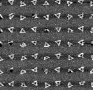
IBM Researchers and collaborator Paul W.K. Rothemund, of the California Institute of Technology, have made advancement in combining lithographic patterning with self assembly – a method to arrange DNA origami structures on surfaces compatible with today’s semiconductor manufacturing equipment.
Today, according to IBM, the semiconductor industry is faced with the challenges of developing lithographic technology for feature sizes smaller than 22 nm and exploring new classes of transistors that employ carbon nanotubes or silicon nanowires.
IBM’s approach of using DNA molecules as scaffolding — where millions of carbon nanotubes could be deposited and self-assembled into precise patterns by sticking to the DNA molecules – may provide a way to reach sub-22 nm lithography, IBM believes.
The utility of this approach lies in the fact that the positioned DNA nanostructures can serve as scaffolds, or miniature circuit boards, for the precise assembly of components – such as carbon nanotubes, nanowires, and nanoparticles – at dimensions smaller than possible with conventional semiconductor fabrication techniques.
This, says IBM, opens up the possibility of creating functional devices that can be integrated into larger structures, as well as enabling studies of arrays of nanostructures with known coordinates.